🧩 Silicon Wafers
Foundation of Modern Electronics
Silicon wafers are thin slices of crystalline silicon that serve as the backbone of the semiconductor industry. They are essential for manufacturing integrated circuits (ICs), solar cells, sensors, and microelectronic devices.
What is a Silicon Wafer?
-
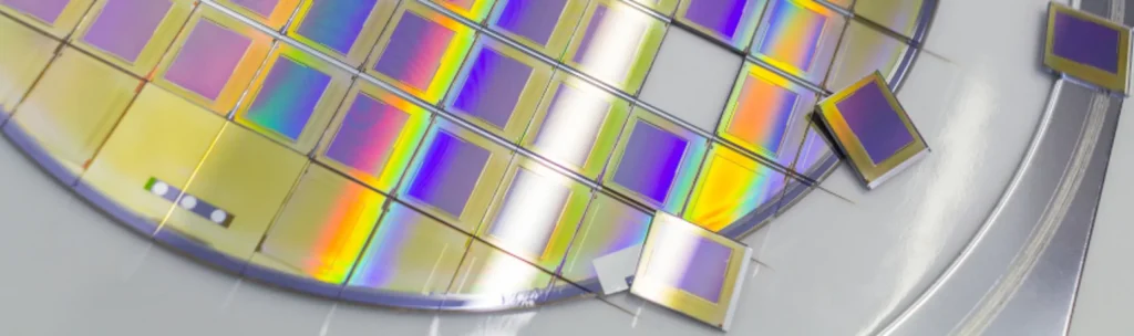
A silicon wafer is a flat, circular disc of highly purified silicon.
-
It acts as a substrate upon which microelectronic components are built.
-
Wafers are polished to extreme flatness and often coated with silicon dioxide for protection
Manufacturing Process
-
Crystal Growth
-
High‑purity silicon is melted and crystallized using the Czochralski method.
-
A seed crystal is pulled from the melt, forming a large cylindrical ingot (boule)
-
-
Wafer Slicing
-
Ingots are sliced into thin wafers using diamond or wire saws.
-
Typical thickness: 100–800 μm depending on application
-
-
Surface Treatment
-
Wafers are polished, etched, and cleaned with acids to remove defects.
-
Doping with boron or phosphorus creates p‑type or n‑type semiconductors
-
-
Oxidation & Layering
-
A thin oxide layer is added for insulation.
-
Additional layers (metals, insulators) are deposited for IC fabrication
-
Types of Silicon Wafers
| Type | Description | Applications |
|---|---|---|
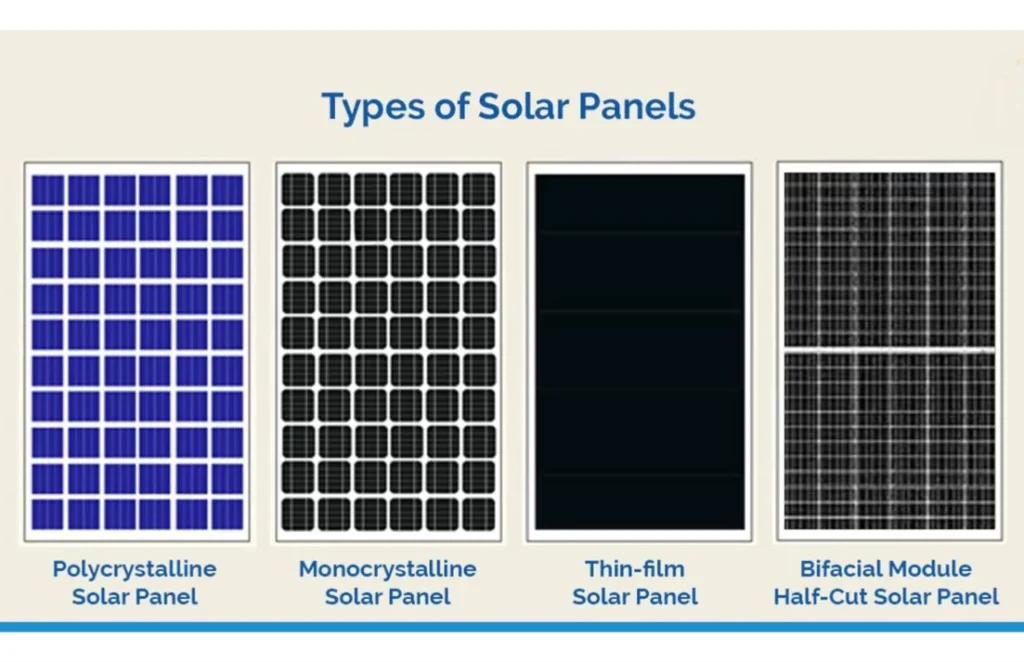
| Monocrystalline | Single crystal, high purity | ICs, high‑efficiency solar cells |
| Polycrystalline | Multiple crystals, lower cost | Solar panels, sensors |
| Epitaxial | Thin silicon layer grown on substrate | Advanced ICs |
| SOI (Silicon‑On‑Insulator) | Insulating layer between silicon | Low‑power, high‑speed chips |
Applications
-
Integrated Circuits (ICs): Basis for computers, smartphones, and electronics.
-
Solar Cells: Convert sunlight into electricity.
-
MEMS Devices: Micro‑electro‑mechanical systems for automotive and medical use.
-
Sensors: Used in aerospace, automotive, and healthcare
Challenges
-
High Energy Consumption: Crystal growth requires extreme heat.
-
Purity Requirements: Needs 99.9999999% (9N) purity for electronics.
-
Cost: Monocrystalline wafers are expensive.
-
Recycling Issues: End‑of‑life wafers and solar panels pose sustainability challenges.